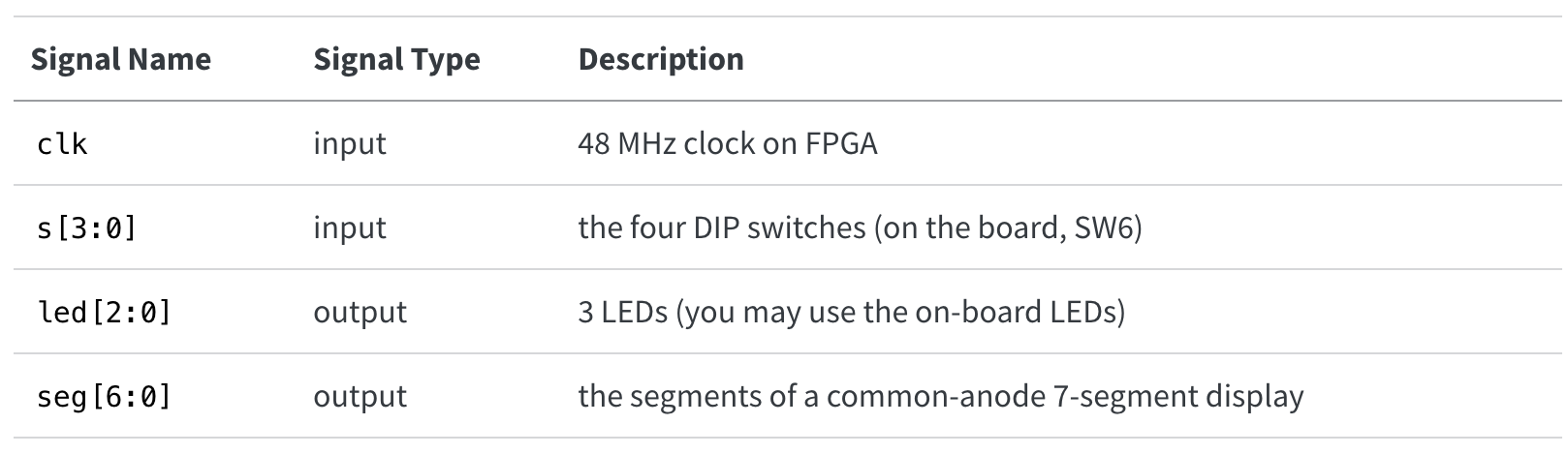
Lab 1: FPGA and MCU Setup and Testing
Introduction
In Lab 1, a development board containing a FPGA (UPduino v3.1) and MCU (mikroBUS_Socket) was soldered together. The objective of the lab was to program the FPGA with Verilog code that responds to 4 input DIP switches and outputs a specific seven segment display as well as three LED displays. Other learning outcomes of the lab consisted of soldering, testing, and debugging circuits and Verilog.
FPGA Design and Testing Methodology.
The following tables from the lab instructions establish the relationship between the various inputs and outputs on the development board.
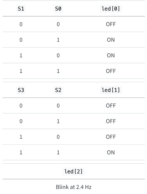
The design was developed using a clock divider, boolean algebra, and multiplexers. The clock divider would create the 2.4Hz oscillating LED, the boolean algebra would select between the DIP switch input signals to determine the other LED outputs, and the multiplexers would select the corresponding segment outputs for the 7-segment display. The 7-segment displays all the hexidecimal digits distinctly.
The 7-segment display has a common anode, meaning that the cathode must be grounding in order to cause the LED to turn on. Therefore, the Verilog code would send a “0” to turn on a segment and a “1” to turn off a segment.
The outputs of the LEDs and 7-segment display would be verified using a self-checking testbench and an oscilloscope trace.
Hardware Implementation
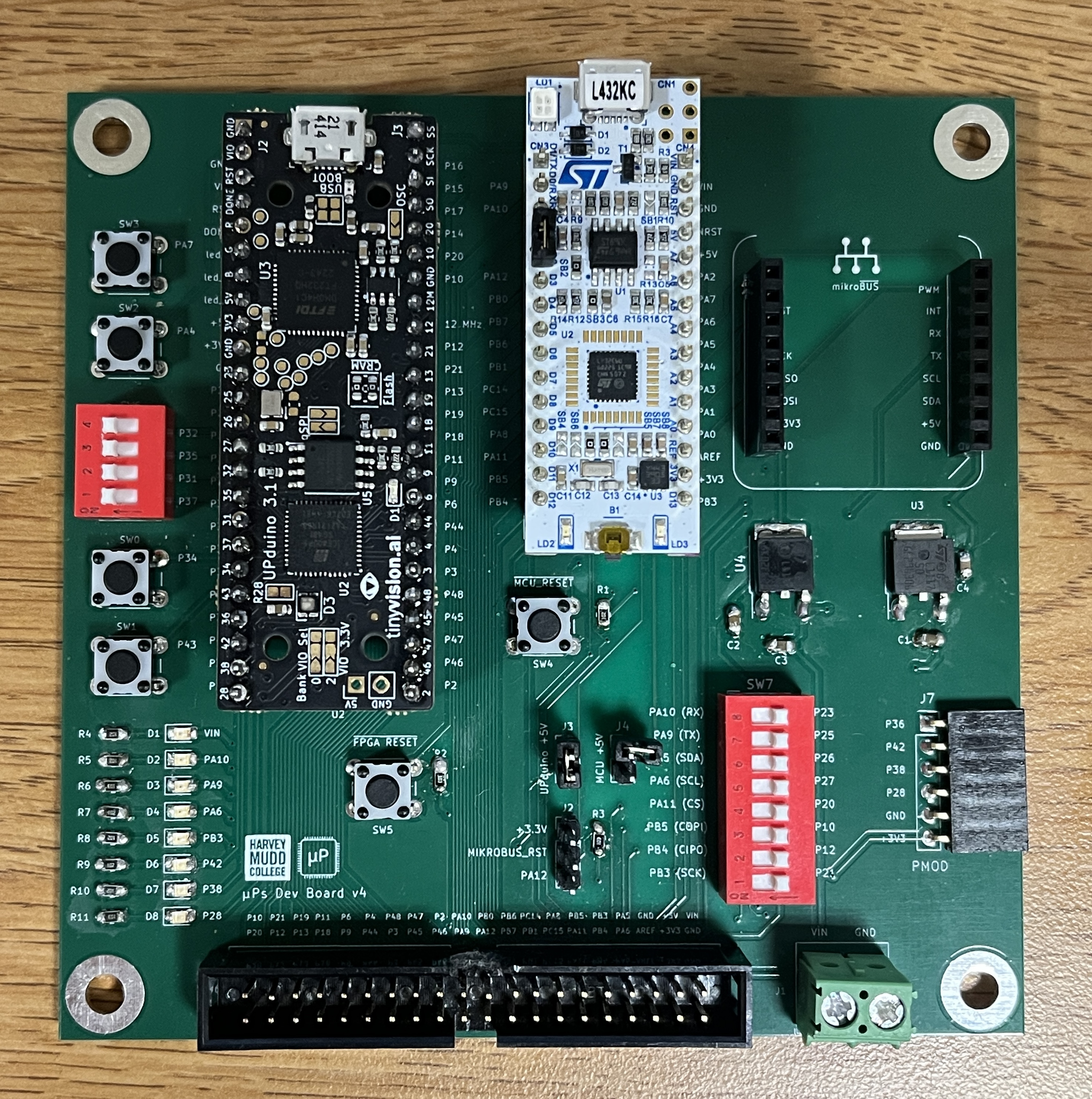
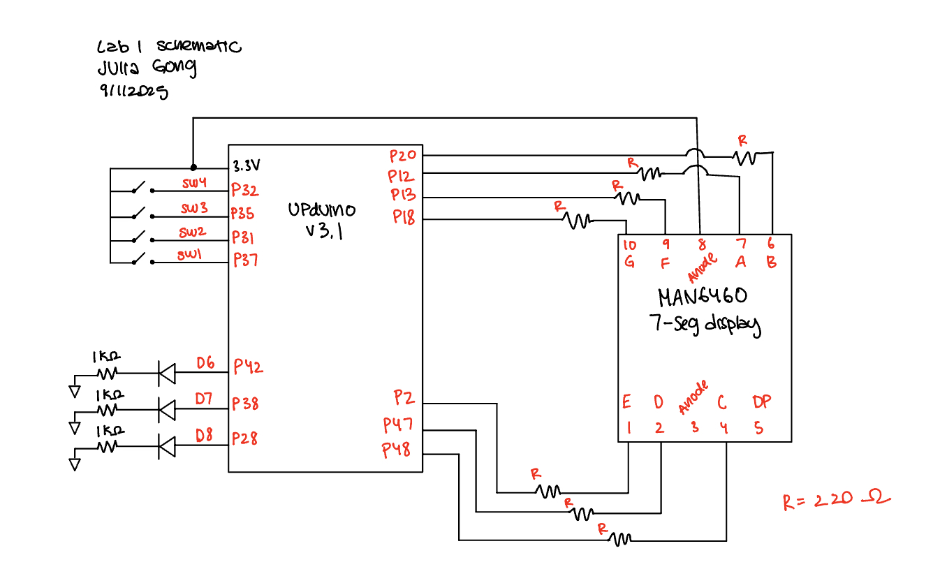
The development board was assembled by soldering votage regulars, SMT components (resistors, capacitors, and LEDs), and various THT components. The schematic of the development board layout can be found here.
The resistors used in the 7-segment display were determined by looking at the segment luminous intensity and voltage drop in the datasheet. From the datasheet, the desired current for the display is 10mA and the voltage drop for the segment is 2.1V. Using the equation V = IR, the desired resistor value for the segment display can be determined. The 7-segment display was supplied 3.3V, so V = 3.3V - 2.1V = 1.2V. After solving for R (resistor value), R was equal to approximately 120Ω. In my design I used 220Ω resistors to ensure that the current drawn from each segment would be appropriate.
Technical Documentation
The source code from this lab can be found in my Github repository. The code contains the two Verilog modules, 2 testbenches (one for each module), and 2 testvector files.
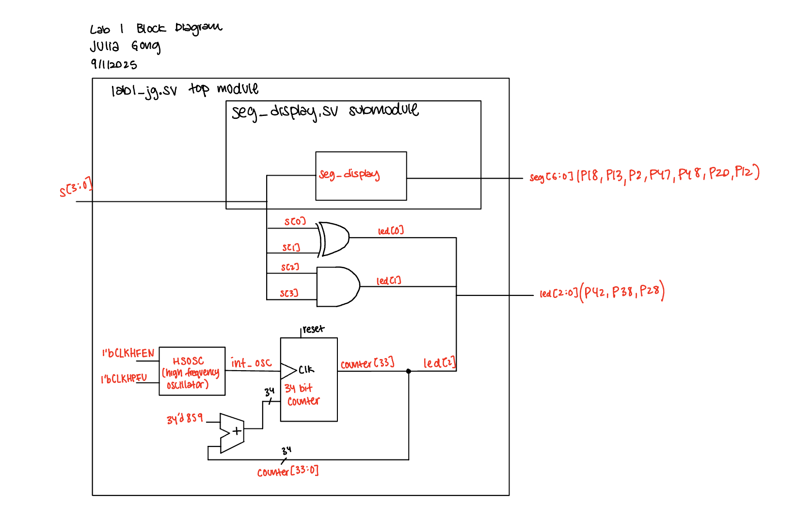
Block Diagram
The block diagram shows the 7-segment display Verilog module, the clock divider, and the overall top module for this lab.
Schematic
The schmatic outlines the FPGA pin assigments for the 4 DIP switches, LEDs, and 7-segment display.
Results and Discussion
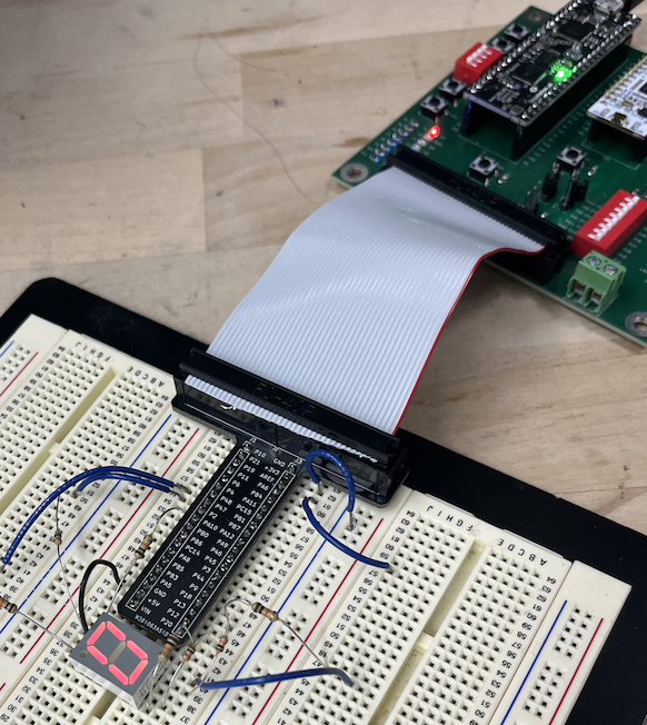
The results of this lab were verified using an automatic testbench simulation on Questa and an oscilloscope trace to verify the LED oscillating frequency. The video below shows the 7-segment display and LEDs responding to DIP switch inputs.
Testbench Simulation
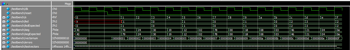
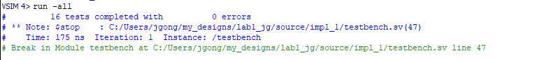
The waveforms and transcript from the Questa simulation show that the expected outputs matched the outputs in the Verilog modules. All 16 tests were completed with no errors.
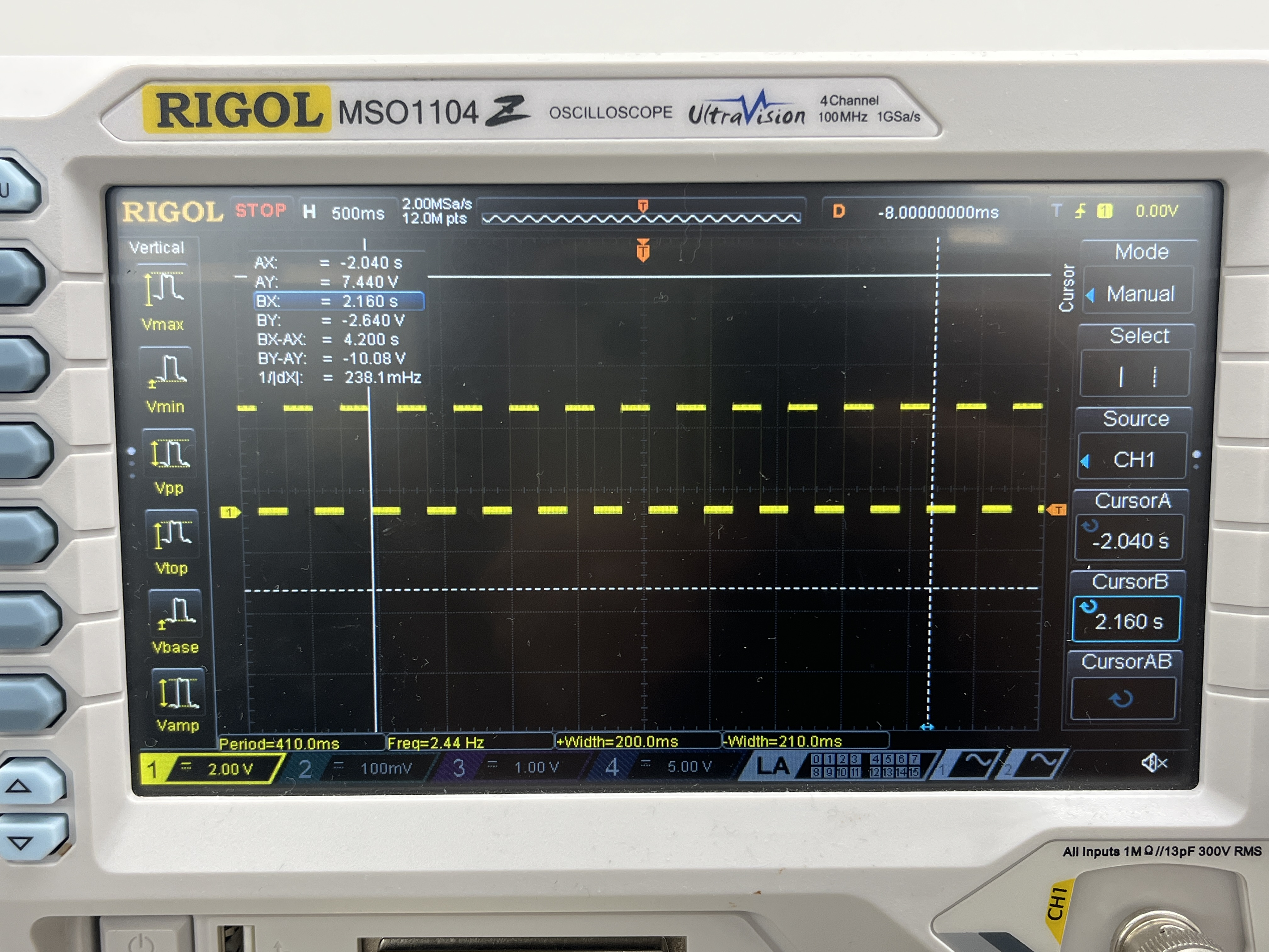
Oscilloscope Trace
The desired frequency for led[2] was 2.4Hz. The oscilloscope trace shows that the measured frequency for led[2] was 2.4Hz.
Conclusion
The design meets all of the requirements for the lab. The development board is completely finished and put together, and the outputs for the 7-segment display and the LEDs all match the expected outputs. All the hexidecimal digits displayed on the 7-segment display are unique, and each segment has the same brightness.
I spent a total number of 15 hours on this lab. A large amount of time in this lab was spent soldering as well as learning about the Lattice Radiant enviroment. There were many small errors I made along the way as well as specific details about Lattice Radiant that could have been helpful to know about in the Lab 1 description. A tip that could have been very helpful would be how to navigate the “FTDI Error” that occurs when trying to program the FPGA.
AI Prototype Summary
For the AI Prototype, I gave ChatGPT the following prompt: Write SystemVerilog HDL to leverage the internal high speed oscillator in the Lattice UP5K FPGA and blink an LED at 2 Hz. Take full advantage of SystemVerilog syntax, for example, using logic instead of wire and reg.
The code that ChatGPT generated included several local parameters in order to cause the LED to blint at 2Hz. I do think the code produced by ChatGPT included a lot of unnecessary parameters, and the logic could be improved/simplified. The output also provided lots of detailed comments about the code as well as information With more guidance and specificity, I do think that ChatGPT could generate better code. After providing more context, with another prompt, ChatGPT was able to produce better code.
The transcript of the chat, including the code generated, can be found here.