MCU Design
Overview
The main purpose of the MCU in this project, STM32L432KC, is to serve as the front-end data acquisition system for the music transcriber. Utilizing a hardware timer triggered Analog-to-Digital Converter (ADC) with double buffers, the system samples analog audio signals, convert them to digital signals, and transmit data packets to the FPGA via SPI. After setting up the required peripherals, the MCU operates in two states, idle and sampling, where the sampling state is triggered and stopped by a button press on the user’s end.
Data Acquisition Architecture
ADC Initialization & Interrupts
The ADC is configured for non-continuous mode and triggered externally by the hardware timer TIM6. The FFT algorithm assumes that the time difference between every single sample is identical. In continuous mode, the ADC samples continuously, starting the next conversion immediately as the previous one finished. Therefore, the sampling time is dependent on internal ADC settings, such as the ADC clock and calibration cycles, making it hard to ensure that the time between samples stay constant and to obtain the sampling frequency. However, by using the non-continuous mode and a timer, the MCU can be set to a desired sampling rate.
The trigger source of the ADC, TIM6, is set to toggle at a frequency of 5 kHz. As the ADC is set to trigger on the rising edge of this timer using Timer 6 TRGO (EXTSEL = 13), a sampling rate of 5 kHz. One important factor in FFT is the frequency resolution, which can be calculated as:
\[ Resolution = \frac{Sampling Rate}{FFT Size} \]
Given that the system uses a 512-point FFT, a higher sampling rate, despite providing more resolution to the original sound signal, would in fact decrease the accuracy of the FFT results. On the other hand, by the Nyquist-Shannon sampling theorem, the sampling rate would limit the highest frequency detectable to be half of the sampling rate. The high C (C6), which is a very high soprano note and hardly appears in pop music melodies, is approximately 1046 Hz. Balancing between the highest frequency detectable, number of data points per period, and the FFT resolution, the sampling rate of the system was decided as 5 kHz.
The resolution of the ADC samples are set to 8-bit instead of the normal 12-bit. The complexity of the math logic gates scales with bit depth on the FPGA. While the iCE40UP5K has DSP blocks, the number of bits of addition and multiplication results quickly grows, and may eventually overflow. Adding more bits to the logics in FPGA was not practical due to the restrictions of resource in the FPGA. 8-bit data would also perfectly fit into one SPI transmission without any extra bits, making the logic of receiving data on the FPGA easier.
Double Buffering
To prevent data loss during the time it takes to transmit data to the FPGA, a double-buffereing method was implemented. Each buffer, buffer0 and buffer1, are set to be 512-byte arrays. fillBuffer acts as a pointer to the array currently being written to by the ADC, and sendBuffer points to the array currently stable and ready for SPI transmission. When the ADC fills fillBuffer with 512 samples, the interrupt handler swaps the pointers and raises a bufferReady flag. The main loop detects this flag and begins transmitting sendBuffer via SPI while the ADC immediately begins writing to the new fillBuffer in the background.
On the other hand, while the STM32 supports Direct Memory Access (DMA), the CPU overhead for processing 5 kHz interrupts is negligible, making the complexity of configuring DMA unnecessary for performance. Additionally, using a standard interrupt allows for simpler, explicit control over the double-buffer pointer swapping logic and easier real-time debugging through GPIO toggles.
SPI Communication
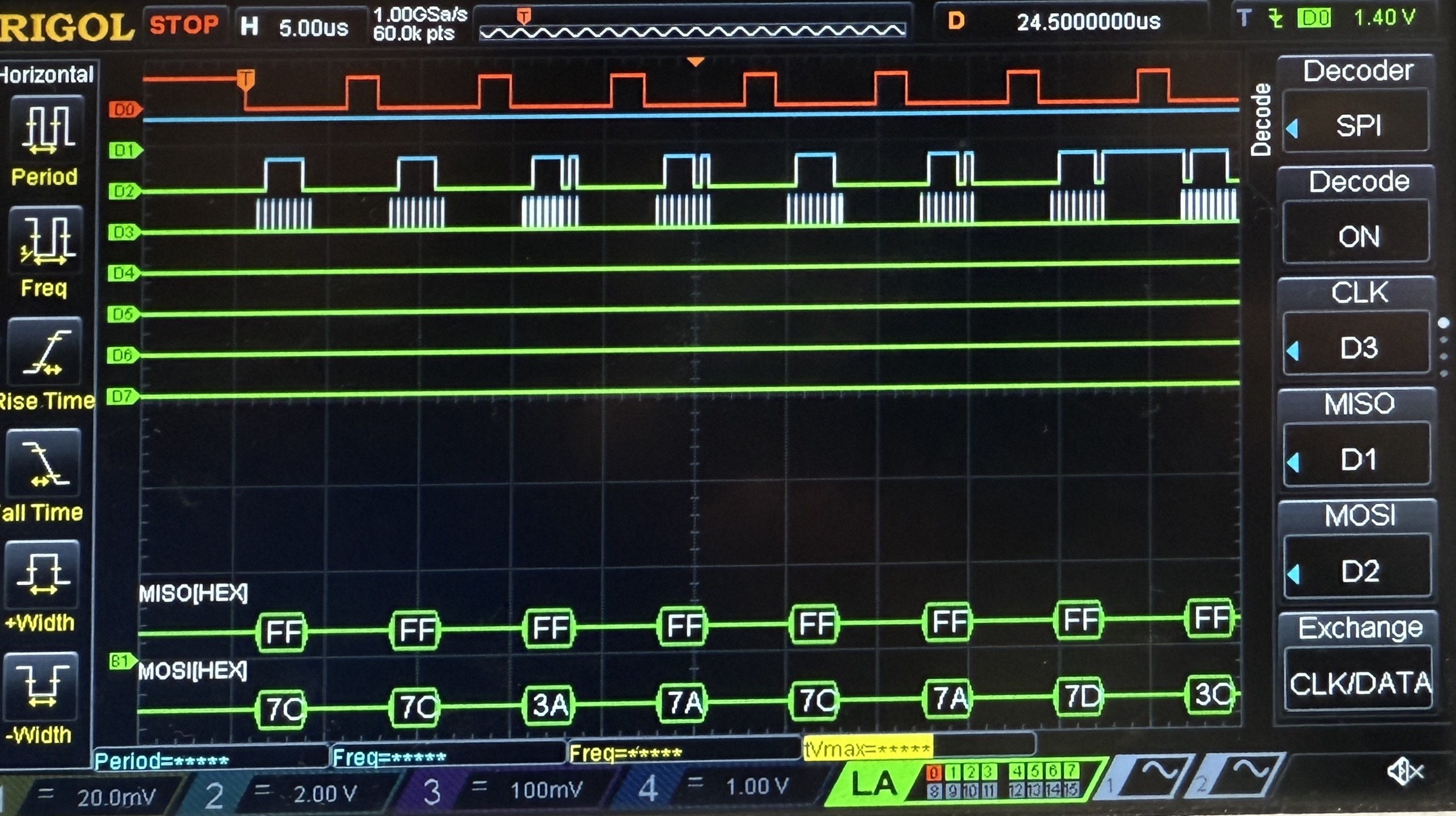
The communication between the MCU and the FPGA is established using the SPI, where the MCU acts as the SPI Master. To ensure synchronization with the FPGA, the Chip Select (CS) line is toggled manually for every byte transmitted. This provides a clear signal for each new “sample” which the FPGA receives.
A logic analyzer result of the SPI transferring the microphone signal is shown here: